Как затеняется PCI ROM?
В нескольких источниках я обнаружил, что: образ ПЗУ должен быть скопирован в ОЗУ на 000C0000h через 000DFFFFh. Если код класса указывает, что это ПЗУ устройства VGA, его код должен быть скопирован в память, начиная с местоположения 000C0000h.
1: Что делать, если у меня есть голодная PCI-карта для бегемота с ПЗУ, размер которого превышает 128 КБ?
2: Что делать, если у меня есть обычное PCI-устройство с ПЗУ 64 КБ, но у меня их 4? Они загружены последовательно в этот диапазон памяти? Если так (хотя я сомневаюсь в этом), как образ кода сохраняется между фазой инициализации и загрузкой?
3: что произойдет, если BIOS решит отказаться от использования и определит другое место в памяти? Почему так или иначе важно использовать этот диапазон?
4: как, черт возьми, обычный случай отличается от интерфейса VGA? Это только предел, который имеет значение?
1 ответ
1: Невозможно скопировать этот большой ROM в дополнительное пространство ROM. Поле размера инициализации составляет 1 байт, и оно интерпретируется как шаг 512 байт, то есть 255 * 512 = 127 КБ
2: Жаль, некоторые из них не будут инициализированы.
3: в северном мосту есть PAM (таблица данных чипсета Intel). Эти регистры могут записывать защищенные определенные диапазоны в дополнительное пространство ПЗУ.
4: Предельные значения для VGA тоже. Он просто должен начинаться с c0000h, в то время как некоторые сетевые адаптеры могут начинаться с.. pfft d0000h.
Спасибо, Пижонг. Добро пожаловать Pyjong.
1) Дополнительные ПЗУ BIOS, не относящиеся к UEFI, обычно не такие большие и имеют ограничения по размеру, но драйверы UEFI могут быть больше и размещаться выше 1 МБ в BIOS UEFI, который переключается из реального режима во время фазы SEC. Вы можете отключить определенные дополнительные ПЗУ, которые не должны быть затенены при следующей загрузке.
3) Этот небольшой диапазон использовался, потому что BIOS, отличные от UEFI, работают в реальном режиме (таблица прерываний (IVT в отличие от IDT) начинается с 0h в качестве гарантии для дополнительных ПЗУ) и, следовательно, может получить доступ только к первым 1 МБ памяти и требует памяти для другие вещи (данные BIOS, BIOS, стек / куча для BIOS и дополнительных ПЗУ). Хотя большинство BIOS в конечном итоге использовали нереальный режим или защищенный режим с виртуальным 8086, поэтому они могли использовать IVT и адрес 32 бита одновременно, поэтому ничто не мешает BIOS затенять дополнительные ПЗУ в другом месте ОЗУ, и BIOS сканирует эту область (Я читал, что E0000–EFFFF также можно использовать, если BIOS составляет всего 64 КБ), за исключением того, что это усложняется, если сами дополнительные ПЗУ ищут другие дополнительные ПЗУ, такие как ПЗУ UNDI, ищущие ПЗУ BC на сетевой карте PxE. Они также использовали PMM службы для выделения адресов кучи размером 16/32 бита. UEFI больше не использует службы прерывания BIOS; он использует функции EFI.
4) Дополнительное ПЗУ для встроенной графики находится в самом BIOS, и его адрес известен. Классически он жестко запрограммирован для перемещения в C0000h (C000:0000h в нотации сегментации реального режима) или даже в другое место. BIOS проверяет, по крайней мере, что это первое дополнительное ПЗУ, которое выполняется, но если он знает, что он переместил его, например, в D0000h, то он знает, где передать управление. Если бы ему было разрешено иметь переменный адрес, а не фиксированный адрес, он мог бы оказаться неспособным вписаться в диапазон, если сначала затеняются другие карты PCIe. Кроме того, ему придется сначала сканировать код класса VGA bios, а затем снова сканировать диапазон или хранить внутреннюю таблицу, где находятся дополнительные ПЗУ, что более запутано, чем простая процедура, которая линейно повторяется в пространстве, а видео BIOS всегда выполняется первым.Таким образом, ему нужен фиксированный адрес, и если он сделает фиксированный адрес D0000h, а не C0000h, и разместит вокруг него другие дополнительные ПЗУ, то произойдет внешняя фрагментация пространства.
Модули PAM больше не находятся в северном мосте (чего нет в современных процессорах Intel), они используются как часть конфигурации SAD в срезе кэша L3, которые декодируют адрес и отправляют запрос в память. контроллер, DMI, канал PCIe или процессорную графику. BIOS может настроить PAM таким образом, чтобы чтение для определенного диапазона отправлялось в DMI, а записи отправлялись в контроллер памяти. Таким образом, BIOS может затенять себя, а панели PCI(e) XROMBAR могут быть настроены на тот же самый адрес, на который они будут затенены.
В моей системе (Kaby lake + PCH серии C230 + безопасная загрузка UEFI отключена) в области C0000h–DFFFFh есть 3 дополнительных ПЗУ.
VGA BIOS
Option ROM Header: 0x000C0000
55 AA 80 E9 91 F9 30 30 30 30 30 30 30 30 30 30 U.....0000000000
30 30 A8 2F E9 B1 2E AF 40 00 90 0B             00./....@...
  Signature 0xAA55
  Length    0x80 (65536 bytes)
  Initialization entry  0x30F991E9 //software read this wrong it's actually 0xF991E9, which is a 16 bit relative jump 0xF991; -1647
  Reserved  0x30 0x30 0x30 0x30 0x30 0x30 0x30 0x30 0x30 0x30
  Reserved  0x30 0xA8 0x2F 0xE9 0xB1 0x2E 0xAF
  PCI Data Offset   0x0040 //offset is from start of OpROM header
  Expansion Header Offset   0x0B90

PCI Data Structure: 0x000C0040
50 43 49 52 86 80 06 04 1C 00 1C 00 03 00 00 03 PCIR............
80 00 00 00 00 80 80 00                         ........
  Signature PCIR
  Vendor ID 0x8086 - Intel Corporation
  Device ID 0x0406
  Product Data  0x001C
  Structure Length  0x001C
  Structure Revision    0x03
  Class Code    0x00 0x00 0x03
  Image Length  0x0080
  Revision Level    0x0000
  Code Type 0x00
  Indicator 0x80
  Reserved  0x0080
Контроллер SATA (заголовок расширения PnP для каждого диска)
Option ROM Header: 0x000D0000
55 AA 4D B8 00 01 CB 00 00 00 00 00 00 00 00 00 U.M.............
00 00 00 00 00 00 00 15 A0 00 9A 01             ............
  Signature 0xAA55
  Length    0x4D (39424 bytes)
  Initialization entry  0xCB0100B8 //mov  ax, 0x100  retf
  Reserved  0x00 0x00 0x00 0x00 0x00 0x00 0x00 0x00 0x00 0x00
  Reserved  0x00 0x00 0x00 0x00 0x00 0x00 0x15
  PCI Data Offset   0x00A0
  Expansion Header Offset   0x019A

PCI Data Structure: 0x000D00A0
50 43 49 52 86 80 2A 28 1C 00 1C 00 03 00 04 01 PCIR..*(........
4D 00 02 0F 00 80 4D 00                         M.....M.
  Signature PCIR
  Vendor ID 0x8086 - Intel Corporation
  Device ID 0x282A
  Product Data  0x001C
  Structure Length  0x001C
  Structure Revision    0x03
  Class Code    0x00 0x04 0x01
  Image Length  0x004D
  Revision Level    0x0F02
  Code Type 0x00
  Indicator 0x80
  Reserved  0x004D

PnP Expansion Header: 0x000D019A
24 50 6E 50 01 02 BA 01 01 06 00 00 00 00 C2 00 $PnP............
D4 00 00 04 01 C4 90 1A 00 00 00 00 00 00 00 00 ................
  Signature $PnP
  Revision  0x01
  Length    0x02 (32 bytes)
  Next Header   0x01BA
  Reserved  0x01
  Checksum  0x06
  Device ID 0x00000000
  Manufacturer  0x00C2 - Intel Corporation  //location 0xD00C2
  Product Name  0x00D4 - SanDisk X400 M.2 2280 256GB //location 0xD00D4
  Device Type Code  0x00 0x04 0x01
  Device Indicators 0xC4
  Boot Connection Vector    0x1A90
  Disconnect Vector 0x0000
  Bootstrap Entry Vector    0x0000
  Reserved  0x0000
  Resource info. vector 0x0000

PnP Expansion Header: 0x000D01BA
24 50 6E 50 01 02 00 00 02 9B 00 00 00 00 C2 00 $PnP............
F5 00 00 04 01 C4 94 1A 00 00 00 00 00 00 00 00 ................
  Signature $PnP
  Revision  0x01
  Length    0x02 (32 bytes)
  Next Header   0x0000 //next PnP expansion header contains nothing useful
  Reserved  0x02
  Checksum  0x9B
  Device ID 0x00000000
  Manufacturer  0x00C2 - Intel Corporation
  Product Name  0x00F5 - ST1000LM035-1RK172
  Device Type Code  0x00 0x04 0x01
  Device Indicators 0xC4
  Boot Connection Vector    0x1A94
  Disconnect Vector 0x0000
  Bootstrap Entry Vector    0x0000
  Reserved  0x0000
  Resource info. vector 0x0000
Контроллер Ethernet
Option ROM Header: 0x000DA000
55 AA 08 E8 76 10 CB 55 BC 01 00 00 00 00 00 00 U...v..U........
00 00 00 00 00 00 20 00 40 00 60 00             ...... .@.`.
  Signature 0xAA55
  Length    0x08 (4096 bytes)
  Initialization entry  0xCB1076E8 //call then far return
  Reserved  0x55 0xBC 0x01 0x00 0x00 0x00 0x00 0x00 0x00 0x00
  Reserved  0x00 0x00 0x00 0x00 0x00
  PXEROMID Offset  0x0020 //RWEverything didn't pick it up as a separate field and made it part of the reserved section so I separated it.
  PCI Data Offset   0x0040
  Expansion Header Offset   0x0060

UNDI ROM ID Structure: 0x000DA020  //not recognised by RW Everything so I parsed it myself
55 4E 44 49 16 08 00 00 01 02 32 0D 00 08 B0 C4  UNDI......2...
80 46 50 43 49 52                                ¦-ÇFPCIR
  Signature  UNDI
  StructLength  0x16
  Checksum  0x08
  StructRev  0x00
  UNDIRev 0x00 0x01 0x02
  UNDI Loader Offset 0x0D32
  StackSize 0x0800
  DataSize 0xC4B0
  CodeSize 0x4680
  BusType PCIR

PCI Data Structure: 0x000DA040
50 43 49 52 EC 10 68 81 00 00 1C 00 03 00 00 02 PCIR..h.........
08 00 01 02 00 80 08 00                         ........
  Signature PCIR
  Vendor ID 0x10EC - Realtek Semiconductor
  Device ID 0x8168
  Product Data  0x0000
  Structure Length  0x001C
  Structure Revision    0x03
  Class Code    0x00 0x00 0x02
  Image Length  0x0008
  Revision Level    0x0201
  Code Type 0x00
  Indicator 0x80
  Reserved  0x0008

PnP Expansion Header: 0x000DA060
24 50 6E 50 01 02 00 00 00 D7 00 00 00 00 AF 00 $PnP............
92 01 02 00 00 E4 00 00 00 00 C1 0B 00 00 00 00 ................
  Signature $PnP
  Revision  0x01
  Length    0x02 (32 bytes)
  Next Header   0x0000
  Reserved  0x00
  Checksum  0xD7
  Device ID 0x00000000
  Manufacturer  0x00AF - Intel Corporation
  Product Name  0x0192 - Realtek PXE B02 D00
  Device Type Code  0x02 0x00 0x00
  Device Indicators 0xE4
  Boot Connection Vector    0x0000
  Disconnect Vector 0x0000
  Bootstrap Entry Vector    0x0BC1 // will be at 0xDABC1
  Reserved  0x0000
  Resource info. vector 0x0000
On another computer with a legacy BIOS, only the VGA option ROM appears in a scan of this region, and at 0xC0000. No EHCI and no SATA. This suggests to me it's embedded in the BIOS but part of the BIOS code and not as an option ROM, which is known as a BAID in the BBS; the code to initialise the controller and scan for boot devices and enter their info in the IPL table and hook int 13h so the MBR/VBR can access the disk is hardcoded in the BIOS. Also, BCV hook order priorities no longer matter because they're all entered into the IPL table as BAIDs anyway nowadays rather than just disk 80h being bootable (populated by reading from the current disk enumeration no. in the BDA and then filling in that many entries with their respective details acquired from int 13h calls). Presumably, the IPL table contains the disk number to boot from and passes it to the vector in the entry which will be the code shared by all BAIDs which loads the first sector from the disk using int 13h to 0x7c00 checks for a valid MBR and then passes control. The MBR will then move itself away from 0x7c00 and load the active partition's VBR to 0x7c00 and pass control to the JMP instruction (if its the default windows one. If its GRUB, it will load and pass control to core.img from sectors 1–65). The VBR will then load the IPL in sectors 1–15 which it locates on the disk using the HiddenSectors value in the BPB in the VBR and passes control to it. On windows, the IPL parses NTFS file system MFT, which immediately follows the VBR, locates bootmgr.exe, decompresses it and passes control to the DOS stub.
The code in the initialisation entry on the SATA controller is a code that far returns 0x100. This appears to have been modified by the BIOS or option ROM itself after the initialisation has taken place, or maybe just a dud because it's an embedded device that is initialised elsewhere in the BIOS. By definition, the initialisation code is now useless and option ROMs that adhere to DDIM may remove the initialisation code from RAM once it has been initialised and recompute the length and checksum. The video bios even does some negative relative jump. This suggests that the BIOS shadows its video BIOS to a location before C0000h, shadowing partially over the VGA VRAM region, such that the option ROM header appears at C0000h.
'length' appears to be describing the amount of space in the legacy option ROM shadow RAM region it takes up after initialisation of the option ROM.
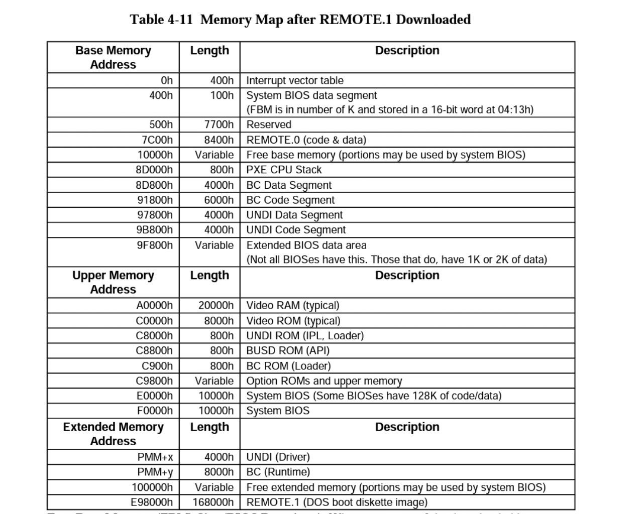
Here is an example memory map of a split PXE option ROM:
Rather than setting all the XROMBARs in one go such that it includes the pre-initialised length, the BIOS probably loads and initialises one at a time. It can't overwrite / remove the option ROM because routines in the option ROM separate to the IPL code may still be called by the BCV to interact with the hardware. For instance, after the video BIOS initialisation code has run, the PCI configuration space is scanned and the first XROMBAR that returns a length will be set to the end of the video BIOS. Reads are then directed to DMI and writes directed to memory. It then shadows it to memory, redirects reads to RAM, and performs a far call to the initialisation entry. The IPL code then shrinks itself by removing the initialisation code. The BIOS checks the new size of the option ROM and for PnP expansion headers and registers BEVs/BCVs. It then redirects loads back to DMI and loads the next XROMBAR. The BIOS builds the BCV table entry at a time and then executes the BCVs in order of BCV priority.
An option ROM could move the BEV/BCV to a PMM allocation in extended memory, leaving a jump instruction at the BEV/BCV offset but that would break relative addressing of jumps in the BCV/BEV into functions in the rest of the option ROM. It could therefore relocate its whole self to a PMM allocation and reduce the size to just the headers, but clearly this isn't the case with most option ROMs. A BEV does relocate the UNDI driver though.